How To Shorten Time To Mass Production Yield Enhancement
Defect teams know that the discovery of bad defects, i.e. root cause analysis for wafer yield, determines wafer yield in a 3nm, 5nm, 7nm and more advanced fab. Limited by the slow SEM image throughput, low defect sample rate makes the discovery of bad defect very difficult. To increase discovery of bad defects, one of the best approaches is to accurately classify and filter nuisance defect as many as possible.
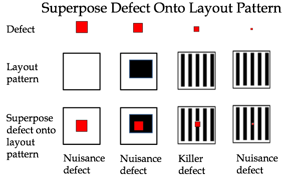
The ESI invention of defect, design layout pattern, and Critical Area Analysis (CAA) (US 8312401) to classify killer defect and nuisance defect accurately is proved to enhance wafer yield and shorten time to mass production successfully in the last few years.